A PCB board is inside almost every electronic device we use, from phones to computers. It connects and supports all the small parts that make the device work. In this guide, I’ll answer the most common questions about PCB boards in clear and simple language.
- Part 1. What is a PCB board used for?
- Part 2. What is a PCB board made of?
- Part 3. What is the function of a PCB board?
- Part 4. What is the difference between PCB and PCBA?
- Part 5. What is the thickness of a standard PCB board?
- Part 6. What is the purpose of a PCB board in electronics?
- Part 7. What is the difference between single-layer and multi-layer PCB boards?
- Part 8. What is a PCB board in a computer?
- Part 9. What is the material used in PCB boards?
- Part 10. What is the importance of PCB boards in modern devices?
- Part 11. FAQs about PCB Board
Part 1. What is a PCB board used for?
A PCB (Printed Circuit Board) is used to mechanically support and electrically connect electronic components. It serves as the backbone of most devices, from smartphones and computers to medical equipment and automotive electronics, ensuring reliable and compact circuitry.
Part 2. What is a PCB board made of?
A PCB is typically made of a base material (substrate) such as fiberglass-reinforced epoxy (FR4), copper foil layers for conductive pathways, and protective layers like solder mask and silkscreen for labeling. Some boards use flexible polyimide or metal cores for special applications.
Part 3. What is the function of a PCB board?
The main function of a PCB is to provide a platform where electronic components are mounted and interconnected. It replaces bulky wiring by using copper traces for connections, ensuring efficient power distribution, signal routing, and mechanical stability in electronic systems.
Part 4. What is the difference between PCB and PCBA?
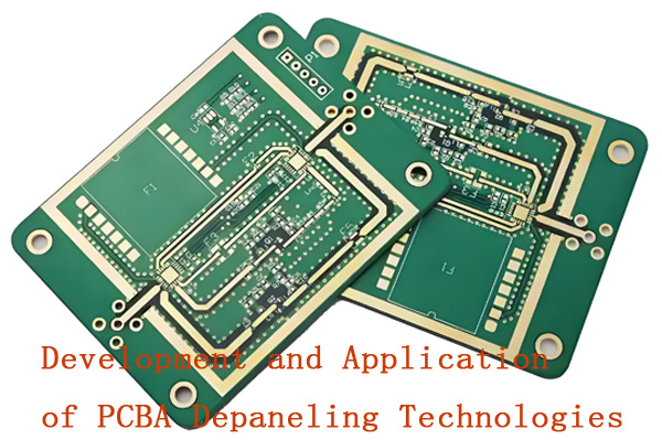
A PCB is just the bare board made of substrate and copper traces, without any components. A PCBA (Printed Circuit Board Assembly) refers to a PCB after electronic components like resistors, capacitors, and ICs are soldered onto it, making it a functional circuit.

Part 5. What is the thickness of a standard PCB board?
The standard thickness for most PCBs is 1.6 mm (0.063 inches). However, thickness can vary from 0.2 mm for flexible PCBs to over 3 mm for heavy-duty or high-power boards, depending on application needs, layer count, and mechanical strength requirements.
Part 6. What is the purpose of a PCB board in electronics?
The purpose of a PCB is to organize and connect components in a compact, reliable way. It provides stable electrical pathways, ensures correct circuit operation, and allows for mass production of electronics, reducing wiring errors and improving efficiency.
Part 7. What is the difference between single-layer and multi-layer PCB boards?
A single-layer PCB has one copper layer for connections, ideal for simple, low-cost circuits. Multi-layer PCBs have multiple copper layers stacked with insulation between them, allowing more complex routing, higher component density, and better performance in advanced devices.
Part 8. What is a PCB board in a computer?
In a computer, a PCB is found in the motherboard, graphics card, and other hardware. It connects the CPU, memory, storage, and peripherals, enabling data flow and power distribution. Without PCBs, modern compact and high-speed computers would not be possible.
Part 9. What is the material used in PCB boards?
Most PCBs use FR4, a fiberglass-reinforced epoxy laminate, for strength and insulation. The conductive layer is copper foil, while solder mask protects traces. Other materials include polyimide (for flexible PCBs), aluminum (for LED boards), and high-frequency laminates.
Part 10. What is the importance of PCB boards in modern devices?
PCBs are essential in modern devices because they allow compact, reliable, and efficient electronic designs. They enable mass production, reduce wiring complexity, and support miniaturization. From smartphones to medical instruments, PCBs power nearly all electronic innovations.
Part 11. FAQs about PCB Board
What is the role of copper in a PCB board?
Copper forms the conductive pathways (traces) that carry electrical signals and power between components, replacing bulky wires and ensuring efficient circuit performance.
What is the difference between rigid and flexible PCB boards?
Rigid PCBs are solid and inflexible, used in computers and TVs. Flexible PCBs bend and twist, making them ideal for compact devices like smartphones and wearables.
What is the cost of making a PCB board?
PCB cost depends on size, layers, material, and quantity. Simple single-layer boards may cost just a few dollars, while complex multi-layer boards can cost hundreds.
What is the difference between FR4 PCB and other PCB materials?
FR4 is fiberglass epoxy, strong and widely used. Alternatives include polyimide for flexible PCBs, aluminum for high-power LEDs, and high-frequency laminates for RF devices.
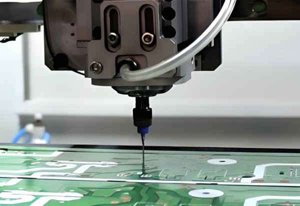
What is the process of manufacturing a PCB board?
It involves designing, printing the cWhat is a PCB board in a mobile phone?ircuit pattern, etching copper, drilling holes, applying solder mask and silkscreen, then testing before assembly.
What is a PCB board in a mobile phone?
It’s the main board that connects the processor, memory, battery, display, and sensors, acting as the phone’s backbone for both power and data flow.
What is the difference between through-hole and surface-mount on PCB boards?
Through-hole components use drilled holes for mounting, stronger but bulkier. Surface-mount parts are soldered directly onto the surface, smaller and ideal for compact designs.
What is the lifespan of a PCB board?
A PCB can last 10–20 years depending on material quality, operating conditions, and usage. Heat, moisture, and stress reduce lifespan.
What is the difference between PCB board layers (2-layer, 4-layer, etc.)?
More layers allow higher circuit density. A 2-layer PCB is simple, while 4–12 layers support complex, high-speed devices with better performance and smaller size.
What is the future of PCB board technology?
Future PCBs will be thinner, flexible, and integrate advanced materials. Trends include 3D printing, high-frequency boards, and eco-friendly substrates for smart, compact devices.
A professional with over a decade of experience in the PCB depaneling industry.