This paper provides an overview of the basic principles, application areas, and key considerations of PCB depaneling technologies. Common depaneling methods include manual break-off, hand snapping, V-scoring, guillotine cutting, routing (milling), punching, and laser cutting.
Modern PCB Panelization Strategies
Electronic products come in various sizes. The final product size determines the PCB dimensions. Compact devices—such as portable electronics, wearables, and board-card modules—use panelized manufacturing. In the industry, this is called “panelization.” A panel contains multiple boards. Each board is called a “piece.”
For example, a “2-up” panel has two pieces. A multi-up panel has more. In smartphones, it is common to use a 4-up panel. This means each panel contains four PCB pieces.
Panel types include mirror panels and identical panels. A 4-up mirror panel has two A-sides and two B-sides. An identical panel uses four A-sides. The term “identical panel” is rare. Most non-mirror panels are simply called “4-up panels.”
Mirror panels were common in earlier production. They allowed both top and bottom sides to be processed on the same SMT line. For example, a panel with two A-sides and two B-sides could go through placement. Then the entire panel could be flipped for another reflow. This made production continuous and efficient, without needing to switch lines.
However, modern complexity has reduced reliance on mirror panels. Critical components like CPUs cannot endure two reflows. Heavy bottom-side modules may fall off during a second reflow. As a result, mirror panels are now rare. They are mainly used for small board-card products.
Identical panels are laid out in two ways. One is step-and-repeat panel. The other is 180° rotated panel. Step-and-repeat panels benefit SMT programming. All parts face the same direction, simplifying placement. Rotated panels benefit boards with connectors. They make better use of board edges.

All panelized boards must be depaneled after assembly. Common depaneling methods include:
●Manual break-off
●Manual snapping
●V-cut
●Guillotine (knife) depaneling
●Routing (milling)
●Punching
●Laser depaneling
Manual Break-Off & Snap Methods
Manual break-off was the earliest depaneling method. It is still used in low-cost appliance PCBs, power supply boards, and consumables. It requires no equipment or jigs. However, it causes high mechanical stress. Boards must have large solder pads and strong mechanical support—such as red-glue single-sided boards. High-density boards or those with ICs should not use break-off.
These panels often use V-grooves. The PCB materials are usually low-strength FR1, FR2, or CEM. Weak mouse bites or bridges can break prematurely. During reflow, boards may warp. Burrs are large and scrap rates increase. This method cannot achieve tight tolerances or clean edges.
Manual snapping is similar to break-off. Sometimes both methods are combined. For example, snap off the panel edge first, then break individual boards. Thin FR4 boards often use snapping. A snap jig supports the board.
Operators must hold the board close to the jig. They should not lift from the top. Lifting from the top creates high torque. This can break solder joints or crack components. Companies should define clear snapping procedures to prevent quality issues.
Manual snapping requires no equipment investment. It relies entirely on labor. It is still used for low-end products. It is prohibited for mid- and high-end products. Burr levels are high and stress is high. This method suits only large, low-cost components and boards where shape and precision are not critical.

V-Cut, Circular Blade, and Guillotine Depaneling
V-cut and blade-based methods are longstanding. Some factories still use them. They reduce stress compared to manual methods. However, they can’t match the low stress of routing.
These methods use circular blades or guillotine knives. V-grooves are made at 30°, 45°, or 60°. Smaller angles yield narrower grooves. Narrow grooves leave more space for components near the edge. A 2.5 mm board with 0.5 mm remaining core will produce a 0.53 mm groove at 30°. It yields a 1.14 mm groove at 60°. Narrow grooves may jam the blade and increase stress.
Narrow grooves require strict tool control. Blade sharpness and blade alignment must be maintained. Tool usage should be logged. PCB panels must lie flat during cutting. This helps reduce stress.
Remaining web thickness depends on material and total board thickness. FR1 or CEM may leave a 1 mm web. FR4 typically leaves 0.4–0.6 mm. It is incorrect to assume web thickness is always one-third of board thickness. A 3.2 mm FR5 board with a 1 mm web is hard to cut with blades. Cutting issues increase. Blade angle and cutting length require careful calculation.

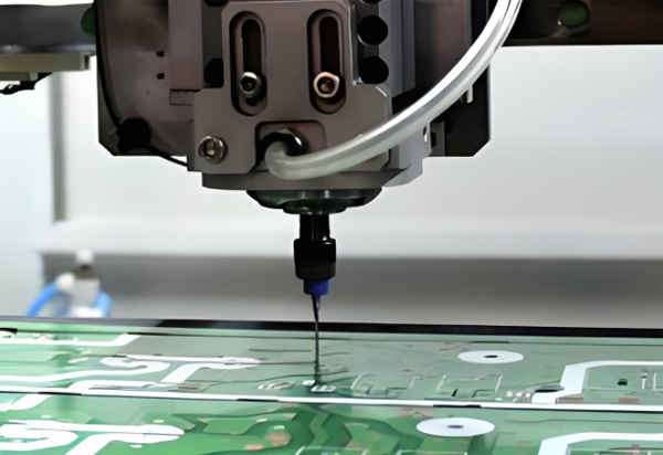
Routing (Milling) Depaneling
Routing is the most widely used method for rigid PCBs today. It employs high‑speed end mills. These mills remove mouse bites or panel bridges.
Routing is available in top-cut and bottom-cut types. Like drilling, it produces debris. In high-density boards—like smartphones or smartwatches—debris can cause problems. For example, debris may affect underfill quality.
Bottom-cut routers are preferred for clean surfaces. Gravity causes debris to fall away. Routers combine vacuum, vibration, ESD brushes, and ion fans to clean debris. High‑cleanliness applications should use bottom-cut routing.
Earlier routers were offline tools. Now, in-line automatic routers are common. They support automatic loading. This includes ESD trolleys, trays, belt feeders, or conveyors. They also include cleaning, edge trimming, and unloading systems.
Fully automated depaneling eliminates manual handling. It avoids fatigue, errors, board mishandling, and Foreign Object Debris (FOD). Noise and environmental conditions are also improved.
Some systems use robots to depanel, test, and sort boards. These systems free up human labor. They enhance factory reliability. Routing stress can be controlled under 300 µε. This makes it suitable for wearables, portable electronics, aerospace, medical, defense, telecom, server, and high-reliability sectors. It delivers precise dimensions and smooth edges.
Routing is notsuitable for metal-core PCBs. Aluminum or copper cores wear out end mills quickly. This increases cost and roughens edge finishes. Stress during cutting also rises.

Punch & Laser Depaneling for FPCs
Flexible PCBs (FPCs) and thin boards use punch or laser methods. Punching was common in earlier FPC production. A die set is made to fit the FPC board. The board is placed in the die and cut. High-end die sets use vacuum to keep FPC flat.
Punching works like scissors. Dull dies cause burrs, board deformation, or cracked solder joints. Dies must be cleaned, maintained, and free of glue, rust, or damage. Boards thicker than 0.5 mm should not be punched. Automation is difficult. Die clearance is limited. Robots struggle to access the die area. Expanding die space affects accuracy and press travel.
For high-volume FPC production, laser depaneling is better. Laser systems can align via fiducial marks. They then laser-cut the FPC. They remove stainless steel carriers, trim edges, unload boards, and recycle carriers—all automatically.
CO₂ lasers are thermal and may cause carbonization. This can lead to leakage in some cases. FPC depaneling needs low-heat cutting. UV lasersare ideal. UV is “cold light.” It minimizes carbonization. It prevents heat-related defects.
UV laser depaneling is fast, precise, and efficient. It needs no fixtures. It supports fully automated production. It is the preferred method for modern high-volume FPC manufacturing.

Laser Depaneling for Metal-Core Boards
Laser cutting also suits metal‑core PCBs. These include aluminum, copper, or aluminum-nitride cores. They are used in Mini LED, Micro LED, lighting, and IGBT modules.
Metal-core boards wear out router tools quickly. Small tools break often. Larger tools reduce material utilization. Milling always remains slow and inefficient.
Laser depaneling is 2–5 times faster than milling. It uses less space on the panel. For example, a 400 × 1200 mm aluminum board yields 5–20% more boards via laser profiling.
After soldering, laser depaneling is ideal. It produces smooth, burr-free edges. It is fully automated. No broken tools. No burrs. It is the preferred choice for metal-core PCB production.
Conclusion
Reducing cost, improving efficiency, cutting labor, and automating production are universal trends. Each automated or digitized process adds value. Electronics manufacturing is complex and precise. Automation and intelligence are inevitable.
The industry has many innovative and confidential solutions. If you face challenges, ask. You might find existing mature solutions. Avoid reinventing the wheel. Innovation is good, but time, cost, and effectiveness matter more. Progress is faster when we build on prior work.
Choose depaneling methods based on product features. The wrong method wastes time and effort.

Example Scenarios:
●A copper-core PCB cut with a router and tungsten-molybdenum bits caused burrs and tool damage. Laser cutting would have been better.
●An IC substrate with quartz-fiber reinforcement could not be cut with a CO₂ laser. It needed routing instead.
No solution is perfect. The right solution isperfect.

A professional with over a decade of experience in the PCB depaneling industry.