When I first started learning about electronics, one of the most confusing yet fascinating parts was PCB manufacturing. In this FAQ, I’ve collected the most common questions people ask about PCB manufacturing—covering everything from how PCBs are made, to costs, testing, certifications, and the latest industry trends.
- Part 1. What is PCB manufacturing process?
- Part 2. How are PCBs made step by step?
- Part 3. What materials are used in PCB manufacturing?
- Part 4. What is the difference between PCB and PCBA?
- Part 5. How long does PCB manufacturing take?
- Part 6. What are the main types of PCBs in manufacturing?
- Part 7. What is the minimum order quantity for PCB manufacturing?
- Part 8. How much does PCB manufacturing cost?
- Part 9. What is the difference between single-layer, double-layer, and multilayer PCBs?
- Part 10. What are common defects in PCB manufacturing?
- Part 11. FAQs about PCB Manufacturing
Part 1. What is PCB manufacturing process?
PCB manufacturing is the process of creating printed circuit boards that connect electronic components through conductive pathways. It involves design, material selection, layering, etching copper traces, applying solder mask, surface finishing, and testing. The process ensures electrical functionality and reliability for use in electronics.
Part 2. How are PCBs made step by step?
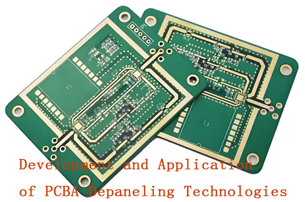
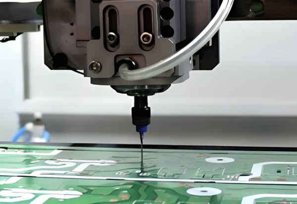
The steps include: circuit design → printing the design on laminate → etching copper to form traces → layering for multilayer boards → drilling holes → plating vias → applying solder mask → printing silkscreen → adding surface finish → electrical testing → cutting/depanneling.
Part 3. What materials are used in PCB manufacturing?
Common materials include FR-4 (fiberglass epoxy laminate), copper foil, solder mask, and silkscreen ink. High-frequency or flexible PCBs may use materials like polyimide, PTFE, or ceramic. The choice of materials affects performance, durability, heat resistance, and cost.
Part 4. What is the difference between PCB and PCBA?
A PCB (Printed Circuit Board) is the bare board made of insulating substrate and copper traces. A PCBA (Printed Circuit Board Assembly) is a PCB that has electronic components soldered onto it. Essentially, PCB is the foundation, while PCBA is the functional, complete circuit.

Part 5. How long does PCB manufacturing take?
Standard PCB production takes about 3–7 days for prototypes and 1–2 weeks for larger runs. Lead time depends on design complexity, number of layers, special finishes, and order size. Expedited services can deliver prototypes in as little as 24–48 hours.
Part 6. What are the main types of PCBs in manufacturing?
The main types are single-layer, double-layer, and multilayer PCBs. Others include rigid PCBs, flexible PCBs, rigid-flex, high-frequency, aluminum-based (for power electronics), and HDI (high-density interconnect) boards. Each type suits different applications.
Part 7. What is the minimum order quantity for PCB manufacturing?
The minimum order quantity (MOQ) depends on the manufacturer. Some allow as low as 1–5 pieces for prototypes, while mass-production factories may require 100 or more. Many PCB service providers now support low-volume or on-demand manufacturing.
Part 8. How much does PCB manufacturing cost?
Cost depends on board size, layer count, materials, surface finish, and quantity. Simple prototypes may cost under $50, while complex multilayer boards can cost hundreds or thousands. Higher volume usually lowers the cost per unit.
Part 9. What is the difference between single-layer, double-layer, and multilayer PCBs?
A single-layer PCB has one copper layer, used in simple devices. A double-layer PCB has copper on both sides, allowing more complex circuits. A multilayer PCB has multiple copper layers separated by insulation, enabling high-density, compact, and powerful electronic designs.
Part 10. What are common defects in PCB manufacturing?
Common defects include open circuits, short circuits, misaligned drilling, poor solder mask application, delamination, insufficient copper plating, and surface contamination. These issues can lead to malfunction, reduced reliability, or failure during assembly.
Part 11. FAQs about PCB Manufacturing
How to choose a PCB manufacturer?
Check quality standards, certifications (ISO, IPC), experience with your PCB type, lead times, pricing, technical support, and customer reviews before deciding.
What is the role of solder mask in PCB manufacturing?
The solder mask insulates copper traces, prevents oxidation, avoids solder bridging, and gives PCBs their characteristic green (or other) color.
What is PCB prototyping in manufacturing?
PCB prototyping is producing small batches of boards to test design, function, and manufacturability before large-scale production.
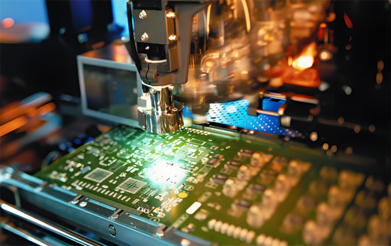
What are the testing methods in PCB manufacturing?
Common methods include Automated Optical Inspection (AOI), Flying Probe Testing, In-Circuit Testing (ICT), and X-ray inspection.
What is the difference between rigid, flexible, and rigid-flex PCBs?
Rigid PCBs are stiff, flexible PCBs bend to fit shapes, and rigid-flex combines both for compact and durable designs.
What is the importance of design for manufacturability (DFM) in PCBs?
DFM ensures PCBs are easy, cost-effective, and reliable to produce by reducing errors and optimizing layouts.
What is surface finish in PCB manufacturing?
Surface finish protects exposed copper, improves solderability, and enhances lifespan. Common types: HASL, ENIG, OSP.
How to reduce PCB manufacturing costs?
Use standard materials, simplify design, minimize layers, order in bulk, and work with manufacturers offering cost optimization.
What certifications are important for PCB manufacturers?
Key certifications include ISO 9001, ISO 14001, UL, and IPC standards (e.g., IPC-6012).
What is the future trend in PCB manufacturing?
Trends include miniaturization, HDI boards, flexible/hybrid PCBs, eco-friendly materials, and integration with AI-driven smart production.
A professional with over a decade of experience in the PCB depaneling industry.