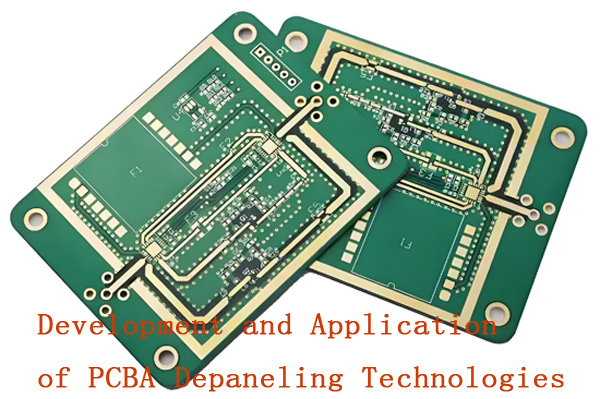
Have you ever looked inside a gadget and seen a green board full of little lines and parts? That’s a PCB—short for Printed Circuit Board. I used to think only big tech companies could make them, but I found out you can actually make one at home! In this simple guide, I answer 20 common questions about how to design, build, and fix a PCB. If you’re just starting with electronics or love DIY projects, this is the perfect place to begin.
- Part 1. How to make a PCB at home?
- Part 2. How to design a PCB layout?
- Part 3. What software is best for PCB design?
- Part 4. How to print PCB design on a copper board?
- Part 5. What materials are needed to make a PCB?
- Part 6. How to etch a PCB?
- Part 7. How to transfer PCB layout to the board?
- Part 8. How to drill holes in a PCB?
- Part 9. How to solder components on a PCB?
- Part 10. How to make a double-sided PCB?
- Part 11. FAQS about Make PCB
Part 1. How to make a PCB at home?
To make a PCB at home, you’ll need to design your circuit, print the layout onto special paper, transfer it onto a copper board using heat (like an iron), then etch the board to remove unwanted copper. After that, drill holes for components and solder them in place. It’s a great DIY electronics project!
Part 2. How to design a PCB layout?
Designing a PCB layout starts with creating a schematic diagram using PCB design software (like KiCad or EasyEDA). Then, you place components and draw copper traces connecting them. Keep spacing rules, signal flow, and power lines in mind. Once done, export your layout as Gerber files for production.
Part 3. What software is best for PCB design?
Popular PCB design software includes KiCad (free and open-source), EasyEDA (web-based and beginner-friendly), Eagle (great for hobbyists), and Altium Designer (professional-grade). The best one depends on your experience level and project complexity.
Part 4. How to print PCB design on a copper board?
First, print the PCB layout (mirror image) onto glossy paper using a laser printer. Then, place the print on a copper-clad board and apply heat with an iron or laminator to transfer the toner. The toner acts as a resist during etching, protecting the copper underneath.

Part 5. What materials are needed to make a PCB?
Basic materials include:
●Copper-clad board (FR4 or phenolic)
●Laser printer and glossy paper
●Etching solution (like ferric chloride or sodium persulfate)
●Soldering tools and solder
●Drill for holes
●Protective gloves and goggles
●Optional: UV exposure unit (for photoresist method)
Part 6. How to etch a PCB?
After transferring the layout to the copper board, submerge it in an etching solution (like ferric chloride). The solution dissolves the exposed copper, leaving only the protected traces. Stir gently and monitor closely. When etching is complete, rinse the board and remove the toner or resist.
Part 7. How to transfer PCB layout to the board?
Use the toner transfer method: print the mirrored layout on glossy or transfer paper with a laser printer. Place it face-down on a copper board and apply heat (iron or laminator) to transfer the toner. Then cool and soak the board in water to remove the paper, leaving the toner on the board.
Part 8. How to drill holes in a PCB?
After etching, use a PCB drill or small rotary tool with carbide bits to make holes for component leads. Hole size depends on your component pins (typically 0.8–1 mm). Use a steady hand or a drill press for accuracy and to avoid cracking the board.
Part 9. How to solder components on a PCB?
Place components in the drilled holes, flip the board, and solder each pin with a soldering iron. Heat the joint, then apply solder to the pin and pad (not directly to the iron). Trim excess leads after soldering. Start with smaller or lower-profile components first for easier handling.
Part 10. How to make a double-sided PCB?
Design both top and bottom layers in your PCB software. Print and align both layers on the copper board. Transfer each side carefully, etch, and drill as usual. Use vias or wires to connect traces between layers. Double-sided PCBs require precise alignment and soldering on both sides.
Part 11. FAQS about Make PCB
How to test a homemade PCB?
Use a multimeter to check for shorts, open circuits, and continuity. Power the board with caution and verify component functions step-by-step.
How to make a PCB without etching?
Use a breadboard for prototyping, or draw traces with conductive ink/pen. Alternatively, use a CNC or pre-made perfboard with wires.
How to make a flexible PCB?
Use polyimide film as the base, print or transfer the circuit, and etch copper foil. Flexible PCBs require special tools and care in handling.
How to create a multilayer PCB?
Stack etched layers with insulating sheets between them. Align, laminate under heat and pressure, then drill and plate vias for connections.
How to clean a PCB after soldering?
Use isopropyl alcohol and a soft brush to remove flux residues. Wipe gently to avoid damaging traces or components.
How to remove toner after PCB etching?
Scrub with acetone or nail polish remover using a soft cloth or brush. Be sure to do it in a well-ventilated area.
How to make PCB using UV method?
Print layout on transparent film, place over photoresist-coated board, expose to UV light, develop the image, then etch.
How to convert a schematic to PCB layout?
Use PCB design software. After drawing the schematic, switch to PCB view to place components and route traces automatically or manually.
How to fix mistakes in a homemade PCB?
Use jumper wires to fix open traces. Cut and rewire faulty connections. For shorts, scrape excess copper or use a knife to isolate areas.
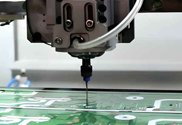
How to make a PCB using CNC machine?
Design the layout in CAM software, generate G-code, and use a CNC router to mill away copper, drill holes, and cut the board outline.
A professional with over a decade of experience in the PCB depaneling industry.