When I first learned how to make a printed circuit board (PCB), the process seemed complicated. But once I understood each step, it became much easier and even fun. In this guide, I’ll walk you through the basics—from using design software and choosing materials to making, testing, and finishing your own PCB—so you can confidently build one yourself.
- Part 1. What are the basic steps to make a PCB?
- Part 2. Which software should I use to design a PCB?
- Part 3. What materials are needed to manufacture a PCB?
- Part 4. What is the difference between single-layer, double-layer and multilayer PCBs?
- Part 5. How do you choose the correct trace width and spacing on a PCB?
- Part 6. What is a PCB Gerber file and why is it needed?
- Part 7. How do vias work and when should you use them on a PCB?
- Part 8. What is the solder mask and silkscreen and how are they applied?
- Part 9. How do you etch a PCB at home safely?
- Part 10. What are the common manufacturing defects in PCBs and how do you avoid them?
- Part 11. FAQs about Make a PCB
Part 1. What are the basic steps to make a PCB?
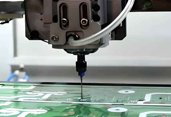
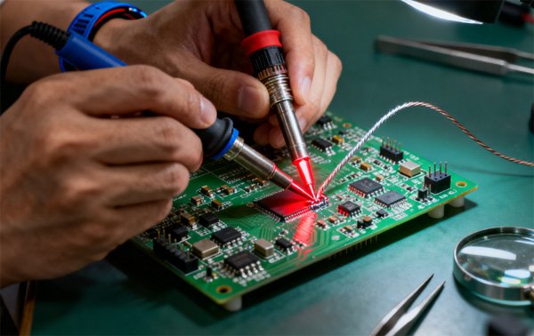
Making a PCB involves several key steps: designing the circuit layout using CAD software, printing or transferring the design to a copper board, etching away unwanted copper to create traces, drilling holes for components, applying solder mask and silkscreen, and finally soldering the components. For professional production, automated machines handle drilling, plating, and quality inspection to ensure precision and consistency.
Part 2. Which software should I use to design a PCB?
Popular PCB design software includes KiCad, Eagle, Altium Designer, and EasyEDA. Beginners often start with KiCad or EasyEDA for their free access and simple interfaces. Professionals prefer Altium or Eagle for advanced features like 3D visualization, DRC checks, and library management. The best choice depends on your project scale, budget, and manufacturing compatibility.
Part 3. What materials are needed to manufacture a PCB?
The main material is copper-clad laminate, typically made of fiberglass epoxy (FR-4) with a copper foil layer. Other essential materials include solder mask ink, silkscreen ink, photoresist, and etching chemicals (like ferric chloride). Conductive vias use copper plating, and for special boards, materials such as aluminum, polyimide, or PTFE are used to improve heat resistance or signal performance.
Part 4. What is the difference between single-layer, double-layer and multilayer PCBs?
A single-layer PCB has copper traces on one side only, suitable for simple circuits. Double-layer PCBs have copper on both sides connected by vias, allowing more complex routing. Multilayer PCBs contain multiple internal copper layers separated by insulation, ideal for high-density and high-speed designs like motherboards or smartphones. More layers mean greater design flexibility and signal integrity.

Part 5. How do you choose the correct trace width and spacing on a PCB?
Trace width depends on the current the conductor carries and the temperature rise allowed. Online calculators (based on IPC-2221 standards) help determine proper dimensions. For low-current signals, 6–10 mil traces are common, while power traces need wider paths. Minimum spacing is often set by the manufacturer’s capabilities, typically 6–8 mil, to avoid short circuits and ensure reliable fabrication.
Part 6. What is a PCB Gerber file and why is it needed?
A Gerber file is the standard format manufacturers use to produce PCBs. It contains all layer data—copper traces, drill holes, solder mask, and silkscreen. Think of it as the “blueprint” of your design. Fabricators load Gerber files into CAM machines to create precise tooling paths. Without Gerber files, a PCB manufacturer cannot accurately reproduce your circuit design.
Part 7. How do vias work and when should you use them on a PCB?
Vias are small plated holes that connect copper layers within a PCB, allowing signals to pass vertically between layers. They are essential in double-sided and multilayer boards. Use vias when routing traces that must change layers due to limited space or to reduce crosstalk in high-frequency circuits. Types include through-hole, blind, and buried vias, each serving different design needs.
Part 8. What is the solder mask and silkscreen and how are they applied?
The solder mask is a protective epoxy layer that covers copper traces, preventing oxidation and solder bridges. It gives the board its color (commonly green). The silkscreen is a printed layer showing component labels, logos, and orientation marks. Both are applied using screen printing or photo-imaging during manufacturing, enhancing appearance, protection, and assembly accuracy.
Part 9. How do you etch a PCB at home safely?
To etch a PCB at home, transfer your printed circuit pattern onto a copper-clad board using toner transfer or photoresist film. Immerse the board in an etching solution such as ferric chloride or sodium persulfate to dissolve unwanted copper. Always wear gloves, goggles, and work in a well-ventilated area. Dispose of used chemicals properly to avoid environmental harm.
Part 10. What are the common manufacturing defects in PCBs and how do you avoid them?
Common PCB defects include open circuits, shorts, solder bridges, misaligned vias, and delamination. These issues often arise from design errors, contamination, or poor process control. To avoid them, follow DFM (Design for Manufacturability) guidelines, ensure clean materials, use proper soldering temperatures, and perform electrical testing (E-test) and AOI inspection before final assembly.
Part 11. FAQs about Make a PCB
How do you test a finished PCB for electrical and connectivity issues?
Use a multimeter for continuity checks, and perform an E-test (flying probe or bed-of-nails) to verify all connections. Advanced testing may include functional tests, AOI, and X-ray inspection for hidden solder faults.
What types of finishes (HASL, ENIG, OSP) exist and how do they differ?
HASL uses solder coating—cheap but uneven. ENIG provides a flat, durable gold surface ideal for fine-pitch components. OSP adds an organic layer protecting copper, great for short-term storage and low-cost assemblies.
How much does it cost to get a PCB manufactured in low volume?
Low-volume PCB costs range from $5–$50 per board, depending on size, layers, finish, and lead time. Simple prototypes (2-layer, small size) are cheapest, while multilayer or quick-turn orders increase price significantly.
How long does it take to go from design to manufactured PCB?
For standard prototypes, manufacturing takes 3–7 days after files are submitted. Complex multilayer or large-volume orders may take 1–3 weeks, especially if surface finishing or testing is required.
How do you prepare and package your PCB files for fabrication (DFM, panelization, etc.)?
Check your design for DFM errors, ensure correct trace widths and clearances, then export Gerber and drill files. Include a readme or fabrication note, verify orientation, and combine small boards into panels for efficient production.