When I first tried making a PCB, I had no idea how many steps were involved—from sketching the design on my computer to seeing that shiny copper board come to life. It’s a surprisingly satisfying process that mixes creativity with precision. I quickly learned that producing a PCB isn’t just about connecting components—it’s about bringing an idea into the real world, one layer at a time.
- Part 1. What are the main steps in PCB manufacturing?
- Part 2. What materials are used to make a PCB?
- Part 3. How is a PCB designed before production?
- Part 4. What software is used to design PCBs?
- Part 5. How are PCB layers created and aligned?
- Part 6. What is the process of etching in PCB manufacturing?
- Part 7. How are vias and holes drilled in a PCB?
- Part 8. How is copper applied or removed during PCB production?
- Part 9. What is solder mask and how is it applied?
- Part 10. How are PCB traces created and protected?
- Part 11. FAQs about Produce a PCB
Part 1. What are the main steps in PCB manufacturing?
PCB manufacturing involves several key steps: design and layout creation, printing the circuit pattern, etching to remove excess copper, drilling holes for vias and components, applying a solder mask, printing silkscreen labels, adding surface finishes, and finally testing the board for continuity and performance.
Part 2. What materials are used to make a PCB?
PCBs are typically made from a non-conductive substrate like FR-4 (fiberglass epoxy), covered with a thin layer of copper foil. Other materials include polyimide for flexible boards, solder mask resin for protection, and silkscreen ink for labeling. The copper provides conductivity, while the substrate offers mechanical strength and insulation.
Part 3. How is a PCB designed before production?
The design process starts with creating a schematic diagram showing all electrical connections. Then, PCB design software is used to lay out the circuit traces, component placements, and vias on multiple layers. Designers follow electrical, thermal, and mechanical rules to ensure signal integrity and manufacturability before exporting Gerber files for fabrication.
Part 4. What software is used to design PCBs?
Popular PCB design tools include Altium Designer, KiCad, Eagle, OrCAD, and EasyEDA. These programs allow engineers to create schematics, route traces, and run design rule checks. They can also generate Gerber files, BOM lists, and 3D previews, which help ensure accuracy before sending the design to manufacturing.

Part 5. How are PCB layers created and aligned?
Each PCB layer—made of copper and insulating material—is laminated together using heat and pressure. Precise optical alignment systems ensure all layers match perfectly. Registration holes and optical targets help align inner copper patterns with outer ones to maintain electrical connectivity and accurate trace routing.
Part 6. What is the process of etching in PCB manufacturing?
Etching removes unwanted copper from the board, leaving only the designed circuit traces. Typically, a photoresist film protects the copper areas meant to remain. The exposed copper is then dissolved using chemical solutions like ferric chloride or cupric chloride, revealing the circuit pattern.
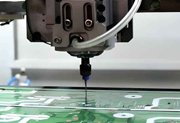
Part 7. How are vias and holes drilled in a PCB?
Vias and component holes are drilled using CNC machines or lasers. Mechanical drills are used for larger holes, while lasers handle microvias in multilayer boards. After drilling, holes are plated with copper to establish electrical connections between layers, a process called through-hole plating.
Part 8. How is copper applied or removed during PCB production?
Copper is applied through lamination of copper foil sheets or electroplating. In subtractive methods, unwanted copper is etched away to form traces. In additive methods, copper is selectively plated only where needed, improving precision and reducing waste in advanced PCB manufacturing.
Part 9. What is solder mask and how is it applied?
Solder mask is a protective epoxy layer applied over the PCB’s copper traces, leaving pads exposed for soldering. It’s applied as a liquid or film, then cured with UV light. The mask prevents solder bridging, oxidation, and contamination, improving both performance and reliability.
Part 10. How are PCB traces created and protected?
PCB traces are formed by etching away excess copper, leaving narrow conductive paths based on the circuit design. These traces are later covered by a solder mask for protection against oxidation and short circuits. Some PCBs also use surface finishes like ENIG or HASL to preserve solderability and durability.
Part 11. FAQs about Produce a PCB
What is the difference between single-layer, double-layer, and multilayer PCBs?
Single-layer PCBs have one copper side, double-layer boards have copper on both sides, and multilayer PCBs stack several layers with internal connections. More layers allow for complex circuits and higher performance but increase cost and production difficulty.
How are PCBs tested for quality and functionality?
PCBs are tested using electrical tests like flying probe and bed-of-nails to check continuity, shorts, and impedance. Visual inspections and automated optical inspection (AOI) detect physical defects such as misalignments or incomplete solder masks.
What equipment is needed to produce PCBs at home?
For DIY PCB production, you need copper-clad boards, etching chemicals, a laser printer (for transferring designs), a drill, and basic soldering tools. Small home setups can make simple single-layer PCBs for hobby projects.
How do manufacturers ensure PCB alignment and registration accuracy?
Manufacturers ensure alignment using optical registration systems and precise drilling references. Cameras and fiducial marks verify that copper layers, vias, and solder masks are correctly aligned before lamination or printing.
What are common defects during PCB production and how to avoid them?
Common defects include misalignment, short circuits, open traces, and solder mask peeling. These can be avoided by using clean materials, proper imaging techniques, and strict process control during etching and lamination.
How is the PCB surface finish applied (ENIG, HASL, OSP, etc.)?
Surface finishes like ENIG, HASL, or OSP protect exposed copper pads. They’re applied after solder masking—ENIG uses gold over nickel, HASL applies hot solder, and OSP uses an organic coating for oxidation prevention and solderability.
How are components mounted after PCB fabrication?
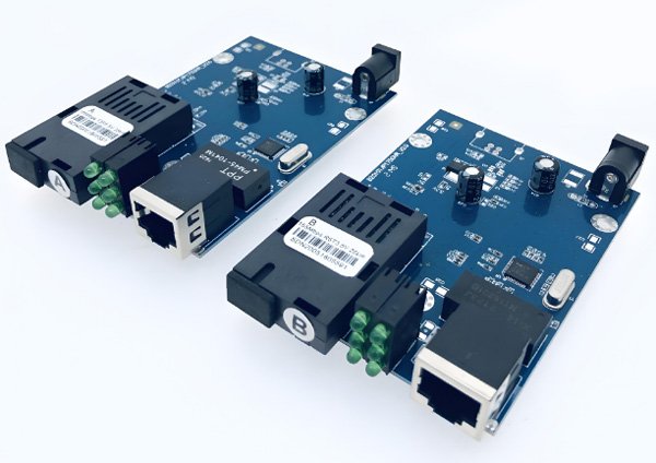
After fabrication, components are mounted using surface-mount technology (SMT) or through-hole soldering. SMT components are placed with automated pick-and-place machines and reflow-soldered for fast, accurate assembly.
How do prototype PCBs differ from mass production boards?
Prototype PCBs are made in small quantities for testing and design verification, often using simpler materials or manual processes. Mass production uses automated, optimized processes for consistent quality and lower per-unit cost.
How long does it take to produce a PCB?
PCB production can take 2–7 days depending on complexity, layer count, and manufacturer workload. Prototypes or expedited services can be completed in 24–48 hours, while complex multilayer boards require more time.
How can I reduce the cost of PCB production without losing quality?
To reduce PCB costs, simplify the layer count, use standard board sizes, avoid tight tolerances, and consolidate orders. Choosing local materials and optimizing trace routing can maintain performance without sacrificing quality.
A professional with over a decade of experience in the PCB depaneling industry.