Many people have heard of PCBs, but not everyone knows how they actually work. In this article, we’ll go over some common questions about the working principles of PCBs. If you’re curious, let’s dive in and learn together!
- Part 1. How does a PCB work in an electronic device?
- Part 2. What is the basic function of a printed circuit board?
- Part 3. How do copper traces on a PCB carry electricity?
- Part 4. How does a multilayer PCB work?
- Part 5. What role do components play on a PCB?
- Part 6. How does electricity flow through a PCB?
- Part 7. How does a PCB connect different components?
- Part 8. What is the function of a PCB substrate?
- Part 9. How does a double-sided PCB operate?
- Part 10. How do vias work in a PCB?
- Part 11. FAQs about How Do PCBs Make Electronics Work
Part 1. How does a PCB work in an electronic device?
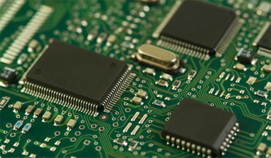
A PCB (Printed Circuit Board) works as the backbone of an electronic device. It holds and connects all the electronic components using copper traces that guide electrical signals. These traces form circuits that allow current to flow between components like resistors, capacitors, ICs, and connectors, enabling the device to perform its intended function.
Part 2. What is the basic function of a printed circuit board?
The basic function of a PCB is to mechanically support and electrically connect electronic components using conductive pathways, or traces, etched from copper sheets. It replaces traditional hand-wiring with a more reliable, compact, and scalable solution.
Part 3. How do copper traces on a PCB carry electricity?
Copper traces act like thin wires embedded into the PCB surface. They carry electric current between components, forming the complete circuit. Traces are designed with specific widths and lengths to control resistance, current flow, and signal timing.
Part 4. How does a multilayer PCB work?
A multilayer PCB consists of multiple layers of copper traces separated by insulating materials. These layers are stacked and laminated together, allowing more complex routing and smaller designs. Internal layers can carry power, ground, or signals independently.

Part 5. What role do components play on a PCB?
Components on a PCB—like microchips, resistors, capacitors, diodes, and connectors—perform specific electrical functions. The PCB connects these components into a working circuit, allowing the device to process signals, store data, power other parts, or communicate.
Part 6. How does electricity flow through a PCB?
Electricity flows through the copper traces, vias, and components on a PCB. Power enters through a power supply, travels along the designed paths, and activates each component according to the circuit logic. Ground planes help complete the circuit loop.
Part 7. How does a PCB connect different components?
A PCB uses copper traces to form pathways that electrically link components placed on the board. These traces connect component pins or pads, guiding signals and power to where they are needed in the circuit.
Part 8. What is the function of a PCB substrate?
The substrate is the base material of a PCB, usually made of fiberglass (FR4). It provides mechanical strength and insulation for the conductive layers. It holds all the copper traces and components in place while resisting heat and moisture.
Part 9. How does a double-sided PCB operate?
A double-sided PCB has copper traces on both the top and bottom layers. Components can be mounted on either or both sides. Vias (plated holes) connect the two layers electrically, enabling more complex routing and higher component density.
Part 10. How do vias work in a PCB?
Vias are small holes drilled through a PCB and plated with copper to allow electrical connection between layers. They enable signals or power to move vertically between layers in double-sided or multilayer PCBs, supporting more compact designs.
Part 11. FAQs about How Do PCBs Make Electronics Work
How do PCBs support signal routing and power distribution?
PCBs use copper traces to route signals and power between components, ensuring controlled and organized electrical paths across the board.
What is the role of ground and power planes in a PCB?
Ground and power planes are large copper layers that distribute stable voltage and reduce electrical noise, improving performance and signal integrity.
How does a flexible PCB function differently from a rigid one?
Flexible PCBs can bend and fold, fitting into tight spaces or dynamic applications, while rigid PCBs remain fixed and are used in standard designs.
How does a PCB reduce electromagnetic interference?
PCBs minimize EMI by using ground planes, controlled trace spacing, and proper layout design to reduce signal noise and crosstalk.
How do PCB layers interact with each other?
Layers are electrically connected using vias and are insulated from each other. They work together to route signals and power in compact designs.
How do PCB traces differ from traditional wiring?
PCB traces are flat, printed copper paths embedded in the board, offering precise, compact, and automated signal routing compared to bulky wires.
How does a circuit get designed to work on a PCB?
Engineers use CAD software to draw the schematic, place components, and route traces, creating a layout ready for PCB fabrication.
How does soldering connect components to a PCB?
Solder melts to bond component leads to copper pads, creating both mechanical attachment and electrical connection on the PCB.
How do surface-mount and through-hole components work on a PCB?
Surface-mount parts sit on the board’s surface, while through-hole parts have leads inserted into drilled holes—both connect via soldering.
How does a PCB help automate electronic device assembly?
PCBs enable pick-and-place machines to quickly mount components, streamlining assembly and reducing manual labor in mass production.
A professional with over a decade of experience in the PCB depaneling industry.


